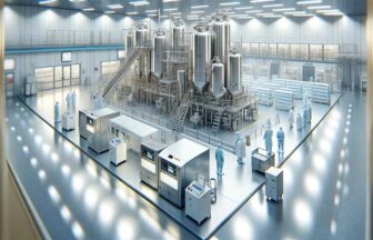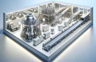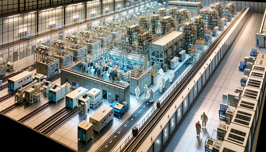
超LSI(超大規模集積回路)の製造は、非常に高度で精密なプロセスを要します。製造にはクリーンルームが必要で、埃や他の微粒子からチップを保護するために超清浄な環境が確保されています。主な製造工程には、フォトリソグラフィ(露光)、エッチング、ドーピング(不純物の添加)、そしてパッケージングが含まれます。これらのプロセスは、非常に高い精度で行われ、回路の微細化と性能向上を実現しています。ULSIチップは、コンピューター、スマートフォン、その他の電子機器の中核となる部品です。
Ultra-large-scale integration (ULSI) chip manufacturing involves highly advanced and precise processes. The production requires clean rooms to protect the chips from dust and other micro-particles, ensuring an ultra-clean environment. Key manufacturing steps include photolithography (exposure), etching, doping (adding impurities), and packaging. These processes are carried out with extreme precision, enabling miniaturization and performance enhancement of circuits. ULSI chips are central components in computers, smartphones, and various electronic devices.